ByJohn A
Protecting and Optimizing Solar Arrays: Diodes and Inverter Component Choices
Solar photovoltaic (PV) systems operate under some of the most unforgiving environmental conditions imaginable. Positioned outdoors for decades, solar arrays are constantly exposed to severe temperature fluctuations, intense UV radiation, and sudden electrical transients. While solar panels capture light and generate direct current (DC), the overall reliability, efficiency, and safety of the installation depend on the discreet semiconductor components managing current flow within the panels and transforming power at the inverter stage.
Optimizing a solar array requires a two-fold engineering strategy: protecting individual PV cells against localized damage and selecting high-efficiency power semiconductors for the inverter conversion stage.
Protecting PV Strings from Shading and Thermal Stress
Solar panels are built from interconnected series strings of silicon photovoltaic cells. Under uniform sunlight, every cell generates a similar voltage and current. However, real-world operation inevitably involves partial shading caused by passing clouds, nearby trees, dust accumulation, or structural obstructions.
The Dynamics of Cell Shading and Hot Spots
When a single cell in a series string is shaded, its current-generating capability drops sharply. Because the unshaded cells in the string continue pushing current, the shaded cell is forced into reverse bias. Instead of generating power, it acts as a resistive load, absorbing energy from the rest of the string and converting it into heat.
This localized heating creates what engineers call a “hot spot.” Unchecked thermal stress from hot spots can burn protective backsheets, crack glass covers, melt solder joints, and permanently degrade panel output.
Bypass and Anti-Reverse Protection
To mitigate shading risks, solar engineers integrate dedicated protective diodes directly into panel junction boxes:
- Bypass Diodes: Connected in parallel across groups of solar cells (typically every 18 to 24 cells), bypass diodes remain reverse-biased during normal operation. When a section experiences shading and drops into reverse bias, the bypass diode conducts, providing a low-resistance path for current to bypass the affected section. This protects the shaded cells from destructive hot-spot formation while keeping the remainder of the panel operational.
- Blocking (Anti-Reverse) Diodes: Installed in series with solar panel strings or battery storage connections, blocking diodes prevent reverse current flow from draining batteries or flowing back through inactive panels during nighttime or heavily overcast conditions.
Designing reliable solar arrays requires choosing high-current, low-forward-voltage components. Engineers evaluating panel protection strategies can consult a comprehensive guide on photovoltaic diodes to match forward current (IF) ratings and thermal dissipation limits to specific module layouts.
Inverter Architecture: Converting DC to Grid-Ready AC
Once solar panels generate DC power, that energy must be stepped up, stabilized, and converted into synchronized alternating current (AC) for grid delivery or local consumption. The PV inverter handles this complex conversion via distinct power stages, each placing specific demands on discrete semiconductors.
Boost Stage and Maximum Power Point Tracking (MPPT)
Because sunlight intensity changes throughout the day, string voltages fluctuate continuously. The input stage of a solar inverter utilizes a DC-DC boost converter driven by fast-switching power transistors to maintain an optimized, elevated DC bus voltage while continuously tracking the maximum power point (MPP).
The Inverter Bridge Stage
The core conversion from DC to AC occurs within an inverter bridge (such as a full H-bridge or three-level neutral point clamped topology). Here, high-voltage switching devices rapidly toggle to generate a pulse-width modulated (PWM) waveform that is filtered into a clean sine wave.
Key device selection criteria for the inverter bridge include:
- Low Conduction Losses: Minimizing forward voltage drops (VCE(sat) or VDS(on)) to keep operational efficiency above 98%.
- Fast Switching Response: Reducing switching losses during PWM modulation to enable smaller external filter inductors and capacitors.
- High Thermal Endurance: Ensuring stable performance under high internal enclosure temperatures.
Evaluating supplier quality and component specifications is essential when choosing discrete devices. For a deeper breakdown of topology design choices, engineers can review this detailed solar inverter components guide to streamline procurement and component matching.
Balancing Active Switches: MOSFETs, IGBTs, and Diodes
Selecting the right active switch depends primarily on the operating voltage and switching frequency of the inverter topology.
| Application Stage | Preferred Component | Key Selection Rationale |
| Low-Power / Microinverters | Power MOSFETs | Low RDS(on) and high-frequency capability for ultra-compact designs. |
| High-Voltage String Inverters | High-Voltage IGBTs | Superior conductivity modulation offering low conduction losses at 600V–1500V DC levels. |
| Freewheeling Paths | Fast Recovery Diodes (FRDs) | Ultra-short reverse recovery time (trr) to prevent inductive switching voltage spikes. |
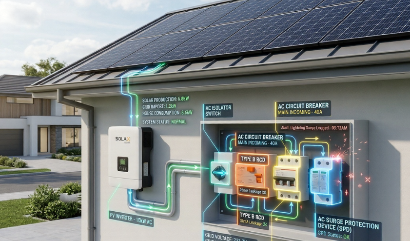
| Grid / Control Line Protection | TVS Diodes | Fast clamping response to shield sensitive DSP controls from lightning and grid surges. |
While power switches dominate efficiency discussions, freewheeling diodes paired across switching devices play an equally vital role. During inductive switching intervals, these fast recovery or Schottky diodes dissipate stored energy safely, preventing voltage transients from breaking down the primary switches.
Thermal Management Best Practices
Solar inverters generate substantial heat during peak mid-day generation. Excessive thermal buildup degrades semiconductor junctions, shortens operating lifespans, and triggers protective power derating that reduces daily kilowatt-hour yields.
To maximize system thermal performance:
- Select Low Forward Voltage Drop Devices: Choosing Schottky diodes with minimal VF for bypass and freewheeling stages directly cuts I2R heat dissipation.
- Optimize PCB Surface Mount Pours: Utilize wide copper thermal planes around surface-mount devices (such as SMA, SMB, or D2PAK packages) to transfer heat away from silicon junctions.
- Utilize Direct Heatsink Mounting: For high-power through-hole packages (TO-247) or integrated power modules, ensure low thermal resistance (RJC) using high-performance thermal interface materials (TIM).
See also: How Field Service Business Software Supports Better Job Scheduling
Final Thoughts
Building a resilient solar energy system requires balancing localized module protection with high-efficiency power conversion. Photovoltaic bypass and blocking diodes safeguard delicate solar cells against hot-spot degradation and unwanted reverse current flow during partial shading. At the same time, carefully matched MOSFETs, IGBTs, fast recovery diodes, and TVS protection arrays ensure that the solar inverter operates with maximum efficiency and high surge immunity over years of continuous outdoor service. By rigorously analyzing thermal parameters, switching characteristics, and voltage margins early in the design cycle, engineers can build solar energy infrastructure capable of delivering maximum clean energy reliably and safely.